
PTFE PCB Guide: Materials, Stackup, and Manufacturing
PTFE PCB is used in circuits where standard FR4 can no longer meet signal requirements.
At RF and microwave frequencies, material loss becomes a serious design limit. Impedance stability, phase control, copper roughness, and stackup structure all affect performance.
PTFE-based laminates give designers a lower-loss option for demanding RF applications. They are common in antennas, radar modules, satellite systems, 5G equipment, and microwave circuits.
This guide explains what PTFE PCB is, how it differs from FR4 and Rogers PCB, and how to design a reliable PTFE PCB stackup.
What Is a PTFE PCB?
A PTFE PCB uses polytetrafluoroethylene-based material as the dielectric layer.
Many engineers also call it a Teflon PCB. In PCB manufacturing, the term usually means a high-frequency circuit board built with PTFE-based laminate.
PTFE has a low dielectric constant and low dielectric loss. These properties make it suitable for RF, microwave, and high-speed signal transmission.
However, PTFE PCB is not one fixed material type. Most commercial PTFE PCB laminates use reinforcement or filler materials.
Common PTFE-based PCB materials include:
· Glass microfiber reinforced PTFE
· Ceramic-filled PTFE
· Woven glass reinforced PTFE
· PTFE hybrid laminates
· PTFE and FR4 mixed stackups
Pure PTFE is difficult to process as a PCB material. Reinforcement and ceramic filling improve mechanical stability, Dk control, and manufacturing reliability.
Why PTFE Is Used in High-Frequency PCBs
PTFE PCB solves problems that appear at higher frequencies.
FR4 works well for many digital and industrial boards. Yet its signal loss increases as frequency rises. Its dielectric properties also change more across frequency and temperature.
PTFE-based materials offer better electrical stability for RF and microwave circuits.
Low Dielectric Loss
Dielectric loss describes how much signal energy the material absorbs.
A lower loss tangent means less signal energy turns into heat. This helps RF signals travel farther with less attenuation.
For antennas, filters, and microwave lines, this loss can affect final product performance.
Stable Dielectric Constant
Dk affects impedance, trace width, phase delay, and wavelength.
A stable Dk makes the circuit easier to predict. This matters for RF filters, antennas, phased arrays, and radar boards.
When Dk changes too much, the final circuit may shift away from the design target.
Better Signal Integrity
PTFE PCB supports cleaner high-frequency signal transmission.
It helps reduce insertion loss and phase variation. It also enables tighter impedance control when designers create the stackup correctly.
This makes PTFE useful for:
· 5G RF modules
· Microwave transmission lines
· Antenna feed networks
· Radar front-end boards
· Satellite communication boards
· RF test equipment
Low Moisture Absorption
Moisture can change dielectric behavior and reduce long-term stability.
PTFE has low moisture absorption compared with many common PCB materials. This supports better reliability in outdoor, aerospace, and communication equipment.
Good Chemical and Thermal Resistance
PTFE has strong chemical resistance and a high service temperature range.
Still, PCB reliability depends on more than PTFE itself. Copper foil, bonding films, plating, surface finish, and stackup design also matter.
A good PTFE PCB needs both the right material and the right manufacturing process.
PTFE PCB vs FR4 PCB
Designers select PTFE and FR4 to meet different electrical and manufacturing requirements.
FR4 is widely adopted because it offers mature processing, stable availability, and lower manufacturing cost. PTFE costs more but offers better high-frequency performance.
| Item | FR4 PCB | PTFE PCB |
| Base material | Epoxy glass laminate | PTFE-based high-frequency laminate |
| Main strength | Low cost and easy processing | Low loss and stable RF performance |
| Dielectric loss | Higher at RF frequencies | Lower at RF and microwave frequencies |
| Dk stability | Moderate | Better for RF design |
| Manufacturing difficulty | Standard process | Requires tighter process control |
| Cost | Lower | Higher |
| Typical use | Digital, power, industrial, consumer electronics | RF, microwave, antenna, radar, satellite |
| Best choice when | Cost and standard routing matter most | Loss, phase, and impedance matter most |
Use FR4 when the circuit does not need RF-grade material performance. Use PTFE when signal loss, impedance stability, or phase accuracy becomes critical.

For many designs, a hybrid stackup gives a better balance. Designers can place PTFE on RF layers and FR4 on low-speed control layers.
PTFE PCB vs Rogers PCB
PTFE PCB is a material system. Rogers PCB is a board made with laminates from a specific brand.
PTFE is a material chemistry. Rogers is a material brand.

Some Rogers materials are PTFE-based. Others use different resin systems, such as hydrocarbon ceramic materials.
This distinction matters during material selection.
A customer may ask for a Rogers PCB, but the design may not require PTFE. Another customer may ask for a PTFE PCB, but several material brands may meet the electrical target.
In practice, engineers should define the material by performance requirements:
· Target Dk
· Target Df
· Frequency range
· Board thickness
· Copper type
· Impedance tolerance
· Thermal requirement
· Cost target
· Lead time requirement
The best choice depends on the circuit, not only the material name.
Key PTFE PCB Material Parameters
PTFE PCB design should start with material parameters.
Do not select a laminate only by brand name. The material data must match the electrical and mechanical target.
Dielectric Constant
Dk affects trace width, impedance, wavelength, and phase delay.
Lower Dk usually allows wider RF traces for the same impedance. This can reduce conductor loss and improve manufacturability.
However, Dk must stay stable across frequency and temperature. Stability often matters more than one nominal value.
Dissipation Factor
Df, or loss tangent, affects insertion loss.
Lower Df reduces dielectric loss at high frequencies. This is one key reason designers choose PTFE-based materials.
Df becomes more important as frequency increases.
Copper Foil Roughness
At high frequencies, current flows near the copper surface.
Rough copper increases conductor loss. Smooth copper can reduce loss, especially in microwave circuits.
The trade-off is adhesion. Smoother copper may require better process control to maintain reliability.
CTE
CTE means coefficient of thermal expansion.
PTFE-based materials can move more than standard FR4 during heat cycles. This movement affects drilling, plating, registration, and long-term reliability.
CTE matters in:
· Multilayer PTFE PCB
· PTFE and FR4 hybrid stackups
· Fine-pitch RF modules
· High-temperature applications
· Boards with many plated holes
TCDk
TCDk describes how Dk changes with temperature.
This parameter matters in radar, aerospace, outdoor communication, and automotive RF systems. These products may face large temperature changes during operation.
A poor TCDk value can shift frequency response and phase behavior.
Laminate Thickness
Dielectric thickness directly affects impedance and trace width.
A small thickness change can move impedance away from the target. This is why stackup confirmation should happen before layout begins.
Before routing critical RF traces, designers can build a preliminary layer structure in the PCB Stackup Design Tool.
The tool helps visualize layer order, dielectric thickness, copper weight, and impedance-related parameters.
PTFE PCB Stackup Design
Stackup design controls how PTFE material performs in the final board.
PTFE PCB stackup design requires careful control of dielectric thickness, copper weight, Dk, Df, and impedance targets. Designers can use this PCB stackup design tool to review layer structures, via types, and impedance profiles during early design planning.
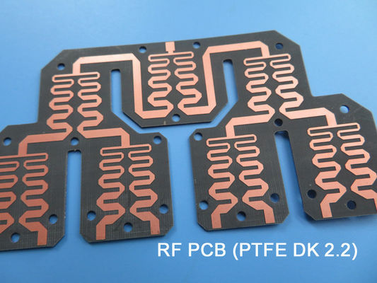
Single-Layer and Double-Sided PTFE PCB
Simple PTFE boards are often used for antennas and microwave traces.
A double-sided PTFE PCB may place RF traces on one side and ground on the other. This creates a microstrip transmission line.
This structure works well for:
· Antenna boards
· RF test coupons
· Simple microwave circuits
· Low-loss transmission paths
· RF sensor boards
The design looks simple, but impedance still needs close control.
Multilayer PTFE PCB
Multilayer PTFE PCB integrates RF, ground, power, and control layers.
It gives designers more routing space and better shielding. It also supports compact RF modules and complex microwave systems.
However, multilayer PTFE PCB brings more manufacturing challenges.
Common risks include:
· Material movement during lamination
· Registration error between layers
· Hole wall preparation problems
· Impedance drift after pressing
· Warpage from unbalanced materials
· Plating reliability issues
A multilayer PTFE stackup should be reviewed before PCB layout starts.
PTFE and FR4 Hybrid Stackup
Hybrid stackups are often the best choice for commercial RF products.
They allow designers to use PTFE only where RF performance matters. FR4 can still support low-speed control circuits, power routing, and mechanical structure.
| Stackup Type | Main Advantage | Main Risk | Best Use Case |
| Full PTFE stackup | Strong RF performance | Higher cost and harder processing | High-end microwave circuits |
| PTFE + FR4 hybrid | Good cost-performance balance | Material compatibility and warpage | RF module with control circuits |
| FR4 only | Lowest cost | Higher RF loss | Low-speed or cost-sensitive products |
Hybrid design should not be treated as simple material stacking.
The engineer must check material expansion, bonding films, copper balance, and lamination behavior.
Symmetric and Asymmetric PTFE Stackups
A symmetric stackup helps reduce board warpage.
Many RF boards become asymmetric because RF layers need special materials. This can create stress during lamination and reflow.
Asymmetric PTFE stackups may still work. They need stronger engineering review before production.
Key review points include:
· Copper distribution
· Core and bonding layer balance
· Total board thickness
· Material expansion behavior
· Pressing conditions
· Surface finish
· Assembly temperature profile
This section can become a strong differentiation point for your article. Many competitors only explain material features, not stackup risk.
Controlled Impedance in PTFE Stackups
Most PTFE PCB projects need controlled impedance.
Common structures include:
· 50Ω single-ended microstrip
· 50Ω coplanar waveguide
· 90Ω differential pair
· 100Ω differential pair
· Stripline between ground planes
· RF launch transitions
For RF traces, ground reference must stay continuous. Any gap, split plane, or poor via transition can create discontinuity.
Designers should also control:
· Trace width
· Trace spacing
· Dielectric height
· Copper thickness
· Copper roughness
· Solder mask effect
· Ground via placement
· Via stub length
The PCB Stackup Design Tool can help create a first stackup model.
PTFE PCB Manufacturing Challenges
PTFE PCB manufacturing requires tighter process control than standard FR4 PCB.
The material behaves differently during drilling, hole preparation, lamination, and plating. These steps affect both reliability and RF performance.
Drilling PTFE Materials
PTFE materials are softer and harder to drill cleanly than FR4.
Poor drilling can cause rough hole walls, smear, or dimensional error. These defects can weaken plating and affect signal behavior.
Drill parameters must match the laminate type. Tool wear also needs close monitoring.
Hole Wall Preparation
PTFE is chemically inert.
This makes hole wall preparation more difficult before copper plating. Poor treatment can cause weak copper adhesion inside plated holes.
Reliable PTFE PCB production needs proper surface activation and process control.
Lamination Control
PTFE multilayer boards need careful lamination planning.
Control pressure, temperature, bonding films, material movement, and layer registration together.
Hybrid PTFE and FR4 stackups need extra attention. Different materials may expand and shrink at different rates.
Copper Adhesion
Copper adhesion is a key manufacturing concern.
Smooth copper helps reduce high-frequency loss. However, smoother copper may reduce mechanical grip.
Manufacturers must balance RF loss and copper bonding reliability.
Dimensional Stability
RF designs can be sensitive to small dimension changes.
A small trace width shift can change impedance. A small dielectric thickness change can also change RF behavior.
This is why PTFE PCB requires tighter fabrication control than normal digital boards.
Surface Finish Selection
Surface finish affects solderability, shelf life, pad planarity, and RF behavior.
Common options include:
| Surface Finish | Advantage | Limitation | Typical Use |
| ENIG | Good shelf life and flat pads | Nickel layer may affect some RF paths | Fine-pitch and general RF boards |
| Immersion Silver | Good conductivity | Needs careful storage | RF and microwave boards |
| Immersion Tin | Flat surface | Shorter shelf life | Selected RF or press-fit designs |
| OSP | Low cost and flat surface | Limited shelf life | Cost-sensitive assemblies |
| HASL | Low cost | Poor flatness for fine pitch | Not ideal for many RF boards |
The right choice depends on RF path design, soldering process, shelf life, and assembly needs.
PTFE PCB Applications
PTFE PCB is used where signal loss and dielectric stability matter.
It appears in communication, aerospace, radar, medical, industrial, and test equipment.
5G Communication
5G systems use high-frequency signals and compact RF modules.
PTFE PCB can support antenna arrays, filters, power amplifiers, and RF front-end circuits.
Common products include:
· 5G base station modules
· Antenna feed networks
· RF front-end boards
· Microwave filters
· High-frequency interconnect boards
Radar Systems
Radar circuits need stable phase and low signal loss.
Automotive radar, industrial radar, and defense radar systems widely use PTFE PCBs.
Phase-sensitive designs need stable Dk and tight impedance control.
Satellite and Aerospace Electronics
Satellite and aerospace systems need reliable RF performance.
These products may face temperature change, vibration, and long service cycles. PTFE materials can support low-loss signal paths in these conditions.
Typical applications include:
· Satellite communication boards
· RF payload modules
· Antenna feed circuits
· Microwave control boards
· Aerospace RF systems
RF Test and Measurement Equipment
RF test boards need repeatable performance.
PTFE PCB helps reduce measurement error caused by material loss and unstable impedance.
Common examples include:
· RF test fixtures
· Microwave test boards
· Calibration circuits
· Signal generator boards
· RF probe interface boards
Medical and Industrial RF Equipment
Some medical and industrial devices use RF energy or high-frequency sensing.
PTFE PCB can support stable high-frequency behavior in these applications.
Examples include:
· Imaging systems
· Wireless medical modules
· Industrial RF sensors
· High-frequency control boards
· Specialized communication modules
PTFE PCB Cost Factors
PTFE PCB costs more than standard FR4 PCB.
The higher cost comes from both material price and process difficulty. Controlled impedance, tight tolerance, and hybrid lamination can also increase cost.
Main cost factors include:
· PTFE laminate type
· Material brand
· Board thickness
· Layer count
· Copper type
· Copper roughness
· Controlled impedance requirement
· Blind or buried vias
· Hybrid stackup complexity
· Surface finish
· Testing requirements
· Production volume
Designers can reduce cost without losing key RF performance.
Practical cost-saving methods include:
1. 1. Use PTFE only on RF layers.
2. 2. Use FR4 for low-speed control layers.
3. 3. Avoid unnecessary blind vias.
4. 4. Use common laminate thicknesses.
5. 5. Confirm the stackup before routing.
6. 6. Set practical impedance tolerance.
7. 7. Avoid over-specifying surface finish.
This helps balance RF performance, lead time, and production cost.
Frequently Asked Questions About PTFE PCB
Is PTFE PCB the same as Teflon PCB?
Many people use these terms in the same way.
PTFE is the material name. Teflon is a well-known brand name related to PTFE materials.
In PCB manufacturing, both terms often refer to high-frequency PCBs using PTFE-based laminates.
Is Rogers PCB always PTFE PCB?
No. Rogers is a material brand, not one material type.
Some Rogers laminates are PTFE-based. Other Rogers laminates use different resin systems.
Always check the actual material data before final selection.
Is PTFE PCB better than FR4 PCB?
PTFE PCB is better for many RF and microwave applications.
FR4 is still better for many standard digital, power, and cost-sensitive boards.
The right choice depends on frequency, loss target, impedance stability, cost, and reliability needs.
Why is PTFE PCB more expensive?
PTFE PCB uses higher-cost material and a more demanding fabrication process.
Drilling, hole treatment, lamination, copper adhesion, and impedance control all need tighter control.
Hybrid stackups and strict tolerances can also increase cost.
Can PTFE be used in multilayer PCB stackups?
Yes. PTFE can be used in multilayer and hybrid PCB stackups.
However, the design needs careful review. Control material compatibility, lamination behavior, registration, and warpage.
What surface finish is best for PTFE PCB?
There is no single best surface finish for all PTFE PCBs.
ENIG, immersion silver, immersion tin, OSP, and other finishes may work in different situations.
The best choice depends on RF performance, solderability, shelf life, assembly process, and pad requirements.