
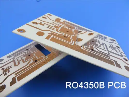
Rogers High Frequency PCB Built On 60mil RO4350B and 6.6mil RO4350B with Immersion Gold for Wireless Booster
Product Description
3 Layer High Frequency PCB Built On 60mil RO4350B and 6.6mil RO4350B with ENIG for Wireless Booster
(PCB’s are custom-made products, the picture and parameters shown are just for reference)
Hi Everyone,
Multilayer high frequency PCBs are made from all high frequency material inclusive of prepreg adhesive. For example, a 4-layer RO4350B PCB is a compound of 2 cores of RO4350B substrates. As is known to all, there’re 8 cores in RO4350B family, i.e. 4mil (0.101mm) to 60mil (1.524mm).
| RO4350B: | |
| 4mil | 0.101mm |
| 6.6mil | 0.168mm |
| 10mil | 0.254mm |
| 13.3mil | 0.338mm |
| 16.6mil | 0.422mm |
| 20mil | 0.508mm |
| 30mil | 0.762mm |
| 60mil | 1.524mm |
So it’s very interesting that stack-up of 4 layers can be done in many different ways.
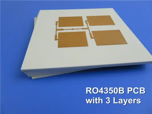
This 3-Layer high frequency PCB is built on 2 cores of RO4350B and one layer of copper is etched off, left 3 layers on.
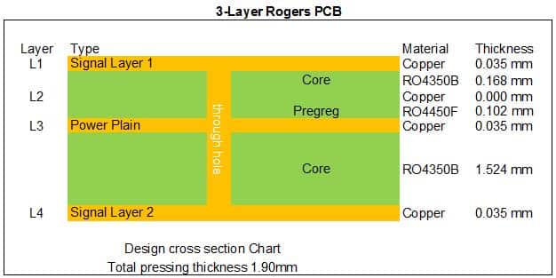
The structure is one sheet of 60mil RO4350B plus 4mil RO4450F prepreg and combined 6.6mil RO4350B. The board is a square with 110mm x 110mm, with immersion gold finishes on pads. They’re 20 pieces packed for shipment and used for wireless booster.
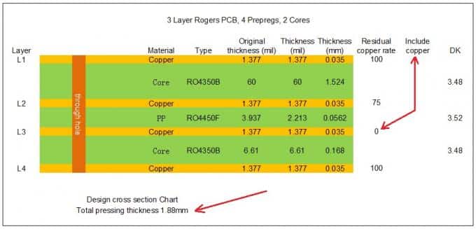
Following is the actual value in engineering manufacture.
Features and benefits
1) Excellent high frequency performance due to low dielectric tolerance and loss;
2) Reducing signal loss in high frequency application meets the development needs of communication technology;
3) Professional and experienced engineers check your production files
4) Hassle-free, one-to-one after-sales service;
5) UL, ISO14001, IAFT16949 certified factory.
Applications
Amplifier, Antenna combiner, Frequency converter, Trunk amplifier, RF module, Power splitter, Low Noise Block, 4G antenna
Parameter and data sheet
| PCB SIZE | 110 x 110mm=1PCS |
| BOARD TYPE | Multilayer PCB |
| Number of Layers | 3 layers |
| Surface Mount Components | YES |
| Through Hole Components | YES |
| LAYER STACKUP | copper ——- 35µm(1 oz)+plate TOP layer |
| RO4350B 60mil (1.524mm) | |
| copper ——- 35µm | |
| Prepreg RO4450F 4mil (0.102mm) | |
| copper ——- 0µm | |
| RO4350B 6.6mil (0.167mm) | |
| copper ——- 35µm(1oz) + plate BOT Layer | |
| TECHNOLOGY | |
| Minimum Trace and Space: | 4 mil / 4 mil |
| Minimum / Maximum Holes: | 0.4 mm / 3.5 mm |
| Number of Different Holes: | 12 |
| Number of Drill Holes: | 124 |
| Number of Milled Slots: | 0 |
| Number of Internal Cutouts: | NO |
| Impedance Control: | no |
| Number of Gold finger: | 0 |
| BOARD MATERIAL | |
| Glass Epoxy: | RO4350B Tg280℃, er<3.48, Rogers Corp |
| Final foil external: | 1 oz |
| Final foil internal: | 1 oz |
| Final height of PCB: | 1.88 mm ±10% |
| PLATING AND COATING | |
| Surface Finish | Immersion gold |
| Solder Mask Apply To: | N/A |
| Solder Mask Color: | N/A |
| Solder Mask Type: | N/A |
| CONTOUR/CUTTING | Routing |
| MARKING | |
| Side of Component Legend | N/A |
| Colour of Component Legend | N/A |
| Manufacturer Name or Logo: | N/A |
| VIA | Plated through hole(PTH), minimum size 0.4mm. |
| FLAMIBILITY RATING | UL 94-V0 Approval MIN. |
| DIMENSION TOLERANCE | |
| Outline dimension: | 0.0059″ |
| Board plating: | 0.0029″ |
| Drill tolerance: | 0.002″ |
| TEST | 100% Electrical Test prior shipment |
| TYPE OF ARTWORK TO BE SUPPLIED | email file, Gerber RS-274-X, PCBDOC etc |
| SERVICE AREA | Worldwide, Globally. |